High Density Interconnector (HDI PCB) Manufacturer in China
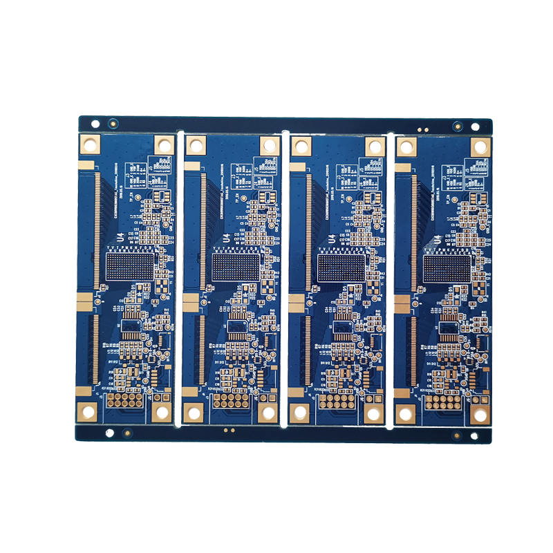
1+N+1 HDI PCB
HDI is High Density Interconnector, which is a technology for producing printed circuit boards. HDI board is a circuit board with relatively high circuit distribution density using micro-blind and buried hole technology. HDI circuit board is a compact product specially designed for small-capacity users. The micro-blind hole annular ring is less than 6mil, the wiring width/line gap between the inner and outer layers is less than 4mil, and the pad diameter is not greater than 0.35mm. Build-up multilayer board production method is called HDI board.
Send Email: fiona@beton-tech.com to Us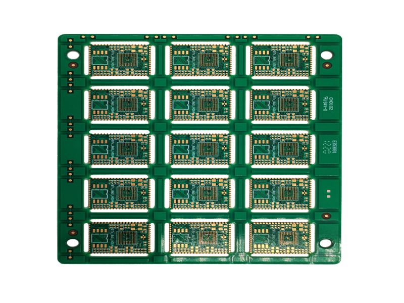
HDI 2+N+2 PCB
HDI (High Density Interconnection) circuit boards usually include laser blind vias and mechanical blind vias; general buried vias, blind vias, stacked vias, wrong vias, cross blind buried holes, through vias, blind via filling plating, thin line small gaps, Pads in microvias and technique to realize the conduction between the inner and outer layers, and usually the diameter of the blind buried is not more than 6mil.
Send Email: fiona@beton-tech.com to Us
3+N+3 HDI PCB
3+N+3 means that the HDI board needs to be laser drilled 3 times, and the upper and lower outer layers are 3-layer PCB. The internal and external traces width should be less than 4mil, and the pad diameter should not be more than 0. 35mm. 3+N+3HDI process requires pressing 4 times and laser 3 times
Send Email: fiona@beton-tech.com to Us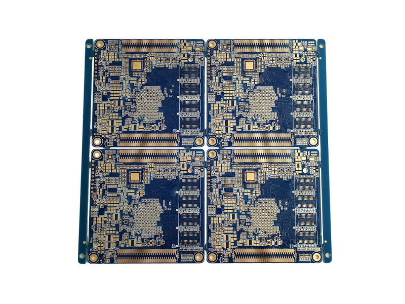
Any layer HDI PCB
The next technological development after HDI microvia PCBs is the use of HDI any layer PCBs, where all electrical connections between layers are made using laser-drilled microvias. Any layer is the highest density plate type in HDI.
Send Email: fiona@beton-tech.com to Us