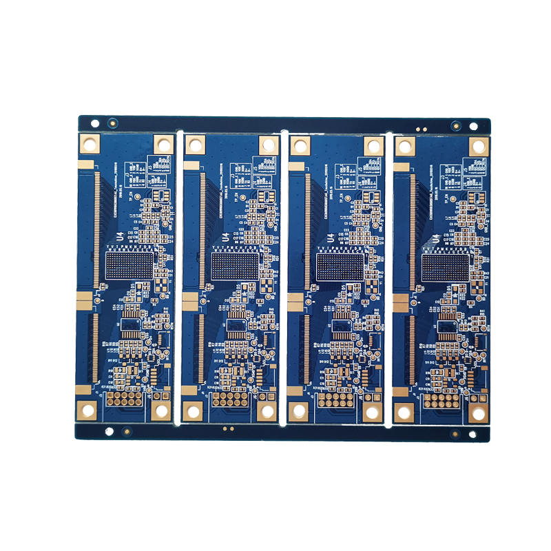
1+N+1 HDI PCB
HDI is High Density Interconnector, which is a technology for producing printed circuit boards. HDI board is a circuit board with relatively high circuit distribution density using micro-blind and buried hole technology. HDI circuit board is a compact product specially designed for small-capacity users. The micro-blind hole annular ring is less than 6mil, the wiring width/line gap between the inner and outer layers is less than 4mil, and the pad diameter is not greater than 0.35mm. Build-up multilayer board production method is called HDI board.
Contact Us Send Email fiona@beton-tech.com to UsBlind holes can realize the connection of Plating through Hole (PTH) between the inner layer and the outer layer
Buried hole can realize the connection of Plating through blind vias to hole large between the inner layer and the inner layer.
Both blind vias and buried vias are 0.05mm-0.15mm small holes. The buried blind vias hole forming methods include laser hole forming, plasma etching hole and photoinduced hole forming. The HDI PCB factory usually used Laser hole forming, and laser hole forming is divided into CO2 and YAG Ultraviolet Lasers (UV).
High Density Interconnector (HDI) PCB Stackup
HDI 1+N+1 is the most basic HDI structure. 1+N+1 means that both the first layer and the last layer need to drill blind holes (usually done by laser drilling). These holes are mainly drilled in the BGA area. There should be enough space in other places. If it is a four-layer board, it will be 1-2 layers and 3-4 layers. If it is a 6 layers board, it will be 1-2 layers and 5-6 layers. As for buried holes, look at it like this not come out.
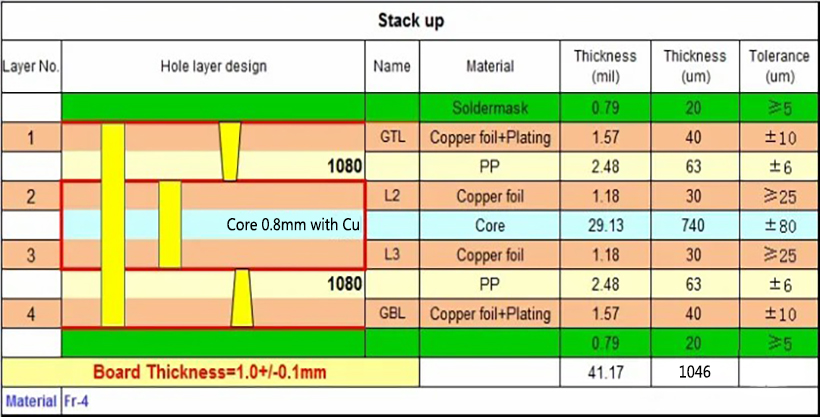
HDI 1+4+1(6 layers) typical Stackup, without buried vias.
Simple six layers first-order HDI (one-time pressing of 6 layers boards, the stackup structure is 1+4+1) There are only through holes and blind vias in the board, but no buried vias. The difference between this situation and the through-hole board is only without blind vias. HDI PCB Stacture needs one press fit, plated blind vias and through holes in production. The difference between six-layer HDI and multi-layer boards is that multiple processes such as laser drilling blind holes are required.
This HDI 1+4+1 stackup structure has no buried holes, so in the production, the 1 layer and 3 layers can be used as a core board, the 4 and 5 layers can be used as another core board, and the outer layer can be added the dielectric PP layer and copper foil. And are laminated together after adding the dielectric PP layer in the middle. This manufacturing simplifies the structure and saves manufacturing costs, and also shortens the production cycle.
HDI 1+4+1 typical Stackup, without through vias.
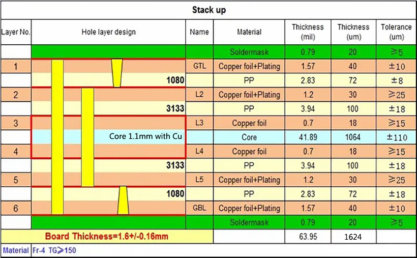
6 layer first-order blind buried via HDI, this HDI PCB board cancels through hole structure. And the 6 layers first-order blind buried via HDI structure needs to be laminated twice, plating the buried vias once, and resin plugged holes once, plating Blind vias once. This HDI structure also saves a certain amount of cost and shortens the delivery time. Please see the follow 1+4+1HDI PCB without through vias stackup.

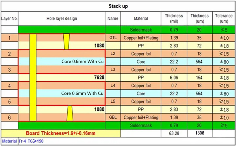
Standard 6 layer HDI 1+4+1 Stackup
Standard 6 layer HDI 1+(Press 6 layers at a time, the stackup is (1+4+1)), this type board stackup is (1+N+1), (N≥2, N is even number), This 6 layers HDI 1+PCB board has through holes, buried vias, and blind vias. This 6 layer 1+ HDI PCB stackup is the mainstream design in the industry. This process is the most complicated, requiring two pressed, once plating buried vias, once resin plug hole, and once plating blind vias and through holes.

More 1+ HDI PCB Stackup
4 layers 1+N+1 HDI (1+2+1) Stackup
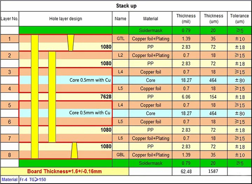
6 layers 1+N+1 HDI (1+4+1) Stackup
8 layers 1+N+1 HDI (1+6+1) Stackup
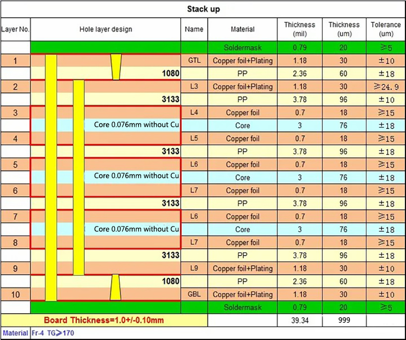
10 layers 1+N+1 HDI (1+8+1) Stackup
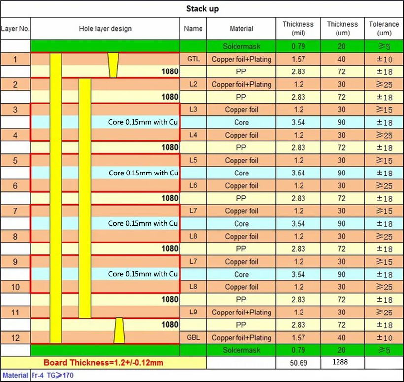
12layers 1+N+1 HDI (1+10+1) Stackup
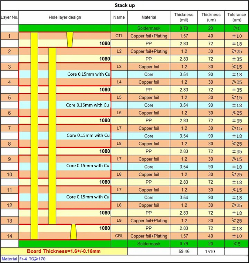
14 layers 1+N+1 HDI (1+12+1) Stackup
High Density Interconnector (HDI) PCB Manufacturing Processing
The 1+ HDI is to drill holes after pressing once, press copper foil once, and laser drill holes. This 1+ HDI board is relatively simple, and the process and process are well controlled. Please check in attachedHigh Density Interconnector (HDI) PCB Manufacturing Processing.

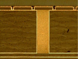
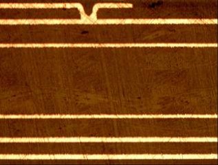
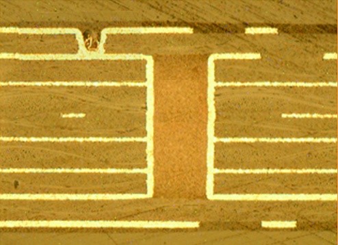
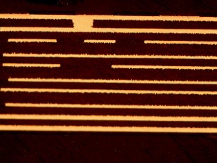
HDI Circuit Board Typical Microsection Diagram (1+N+1)
4 LayersHDI 1+2+1 Microsection |
| 6 LayersHDI 1+4+1 Microsection |
|
|
|
8 LayersHDI 1+6+1 Microsection |
| 1 LayersHDI 1+8+1 Microsection |
|
|
|
1+N+1 HDI boards have been widely used in PCB production with a BGA of 0.5 bits.It is used when the thickness of HDI circuit board FR4 sheet is≤4mil. When using PP, generally use 1080, try not to use 2116 PP. When the customer has no requirements, the copper foil on the substrate is preferably 1OZ in the inner layer of the traditional PCB, the HDI board preferentially use HOZ and 1/3OZ is preferentially used in the internal and external plating layer copper foil.
Any HDI board (High Density Interconnect PCB) project that needs to be produced please email us: Cathy@beton-tech.com. BETON HDI PCBs factory is undoubtedly your best PCB manufacturer choice! BETON HDI PCBs factory with low cost and high quality PCB products, excellent service!