
3+N+3 HDI PCB
3+N+3 means that the HDI board needs to be laser drilled 3 times, and the upper and lower outer layers are 3-layer PCB. The internal and external traces width should be less than 4mil, and the pad diameter should not be more than 0. 35mm. 3+N+3HDI process requires pressing 4 times and laser 3 times
Contact Us Send Email fiona@beton-tech.com to UsThe type III PCB process is much more complicated. First to laminated L3-L6, then L2 and L7, and finally L1 and L8.3+N+3 HDI Board takes 3 lamination times, so most PCB manufacturers can't make it, but our HDI PCB factory has the ability Fabricate a third-order (3+N+3)PCB.
3+N+3 HDI PCBs provide the best stacking configuration for large dense multilayer PCBs using multiple large fine-pitch BGAs. on the inner layers 3+n+3 HDI PCBs use microvias to allow the outer layers to be used for ground and/or power planes for signal routing to leave a sufficient number of layers. In addition, engineering designers can achieve higher routing density by stacking vias.3+n+3 microvia HDI PCB offers the widest range of hole patterns and spans.
3+N+3 HDI PCB Stackup
3+N+3 HDI PCB Stackup may have staggered vias , blind vias stacked vias and Cross-layer blind via. Actually we will adopt the staggered vias stackup design. Because 3+N+3 stackup with staggered vias cost will be cheaper. More engineers will choose the 3+N+3 stackup with staggered vias to reduce the production cost. The Cross-layer blind via design is complicate, so this HDI Boards cost will be higher than other 3+n+3 stackup. But this Cross-layer blind via design has good performance, can meet the requirements of high-tech products
3+N+3 HDI PCB with staggered vias
The 3+N+3 HDI stackup with staggered vias is same as the 2+N+2 HDI. Only the layers lamination times is different.Type III PCB stackup need to connect the next adjacent layer through wires to the middle layer,means three 1+N+1 HDI stackup.

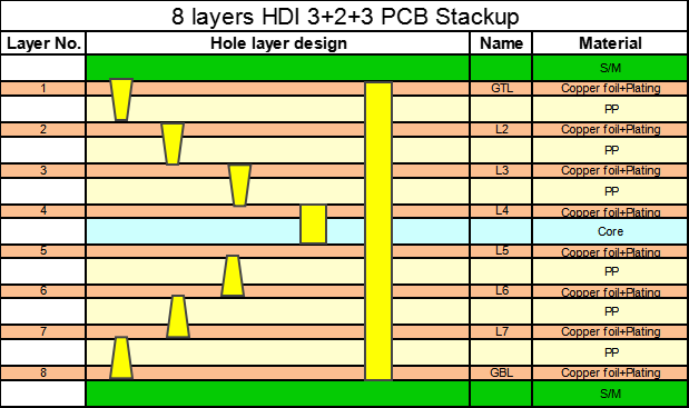
This is the 8 layer 3+N+3 HDI PCB with Staggered vias Stackup. Type III HDI stackup is similar Type III HDI stackup. You can refer to the 2 type stackup.This 3nd Type HDI stackup buried vias in the inner multi-layer board, which needs to be pressed four times to complete. The main reason is that the HDI stackup is no stacked hole design, and the production difficulty is normal. If the L3-L6 buried hole optimize to change to the L2-L7 buried vias, can reduce one pressing , and optimize the process to achieve the effect of reducing costs.
3+N+3 HDI PCB with stacked vias
This is the 3+n+3 HDI stackup with the stacked vias.First to drill the L3-L6 buried vias, then drill the L3-L4, L5-L6 buried vias, and make the L1-l2 blind vias stacked on L3 buried vias. Final to drill the through vias. Please see the following Type III HDI stackup.
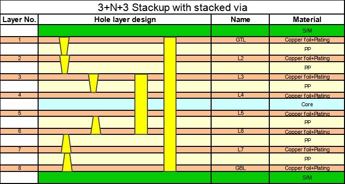
The structure of this type of board is (1+1+1+N+1+1+1), this structure is a 3+N+3 board that is currently difficult to manufacture in the industry, and the inner multi-layer board has buried The holes are in L3-L6, need 4 presses to complete. The main reason is that there are cross-layer blind hole designs, which are difficult to manufacture. It is difficult for HDI PCB manufacturers without certain technical capabilities to make such secondary laminate parts. If such cross-layer blind holes are L1-L3, they can be optimally split into L1- For L2 and L2-L3 blind holes, this method of splitting blind holes is a split method of staggered blind holes, which will greatly reduce the production cost and optimize the production process.
Other 3+N+3 HDI PCB Stackup
8 layers HDI 3+2+3 PCB Stackup
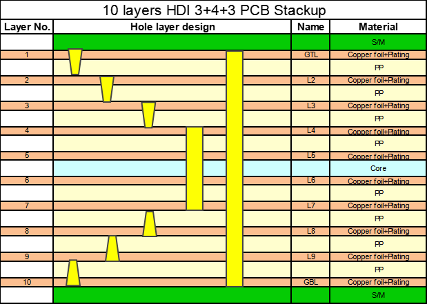
10 layers HDI 3+4+3 PCB Stackup
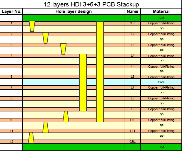
12 layers HDI 3+6+3 PCB Stackup
High Density Interconnector (HDI) PCB Manufacturing Processing
The 3+n+3 hdi stackup process is refer the 2+n+2 process, just add a cycle drilling process based on 2+n+2 process. If you want to know more about the HDI process, please contact us freely.

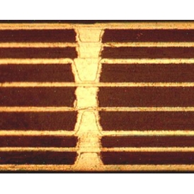
HDI Circuit Board Typical Microsection Diagram (3+N+3)
ThisHDI Circuit Board Typical Microsection Diagramis 3+2+3 HDI stackup.
3+N+3 HDI PCBs provide the best stacking configuration for large dense multi-layer PCBs using multiple large fine-pitch BGAs, although they have the same layer limit as 1+N+1 and 2+N+2 Type faces the same number of layers when using PTH holes and thin FR-4 dielectric.
This Stackup configuration is a good choice for high-density PCBs with multiple layers and using several large BGAs with fine-pitch features. As for FR-4 thin dielectrics and PTH holes, the same restrictions apply.
A significant advantage of the 3+N+3 type is the use of the outer layers as power and ground planes. This can be achieved by placing microvias in the inner layers, ensuring enough layers that manufacturers can use for signal routing.
3+N+3 HDI PCB Advantages
1. Higher wiring density can be achieved.
2. Reduce the area of the pad, reduce the distance from the hole to the hole, and reduce the size of the PCB.
3. Reduce the loss of electrical signals.
High-density integrated HDI technology can make electronic products more miniaturized and meet people's demand for miniaturized electronic products. At present, HDI is widely used in high-end electronic products such as mobile phones and digital cameras.
3+N+3 HDI PCB is also called type III HDI board or 3rd order HDI circuit board. It is a high-level high-density PCB board produced by using micro-blind buried hole technology with relatively high density of circuit distribution. 3+N+3HDI circuit boards are widely used in mobile phones, digital (camera) cameras, MP3, MP4, notebook computers, automotive electronics and other digital products, among which mobile phones are the most widely used. type III HDI is also one of the core competitive products of Beton Circuits, which can provide users with HDI circuit board design, proofing, manufacturing and SMT placement services. You can contact us through our company email cathy@beton-tach.com to learn more about 3+N+3HDI PCB Design.