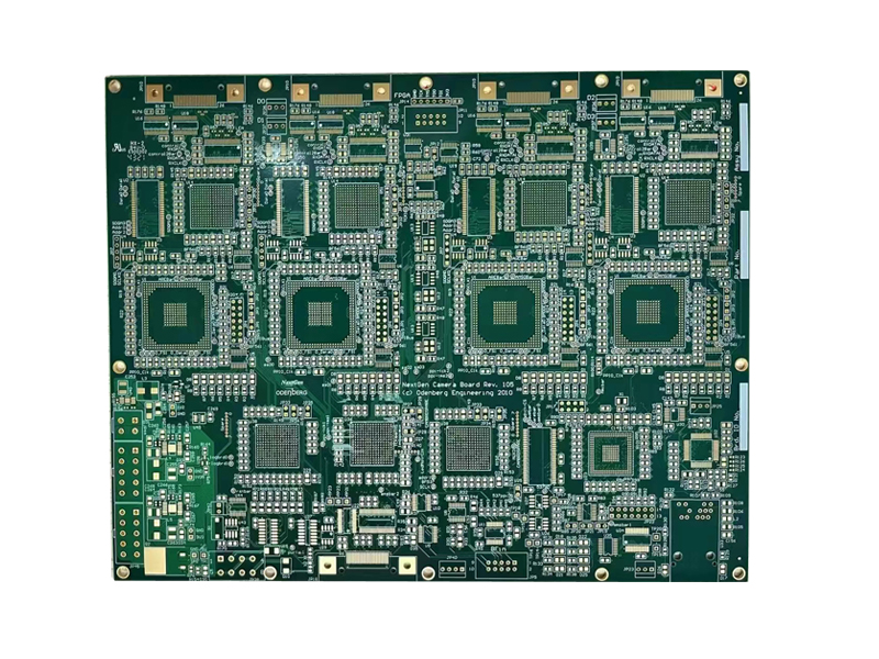
High Density Interconnector(HDI) board
High Density Interconnector(HDI) board is composed of PTH holes (Press fit holes), buried holes and laser drill blind micro-vias holes.
HDI printed circuit board have denser BGA and complicated stack up. Have advantage of light, thin and high density. Our capability can do 1+, 2+, 3+, 4+, 5+ and anylayer HDI PCB, Rigid-flex PCB HDI. Contact Us Send Email fiona@beton-tech.com to UsHDI Fabrication Capabilities
| Item | Fabrication Capabilities |
| The number of layers | 1+,2+,3+,4+, any layer |
| Material | FR-4, High TG FR-4 , Halogen Free material, KB, ITEQ,ShengYI,PTFE,Rogers ,Arlon ,Taconic,Teflon,etc. |
| Maximum PCB Size | 650*1500mm |
| Board Size Tolerance | ±0.2mm/±0.5mm |
| Board Thickness | 0.1-3.2mm |
| Gold Finger Thickness | Normal:0.025-1.27μm Best:1.27-1.51μm |
| Resin Fill | min./max hole size:0.2/1.0mm |
| Max Hole Desity | ±0.075mm |
| Outer Layer Copper Thickness | 1-10oz(35-350μm) |
| Inner Layer Copper Thickness | 0.5oz-10oz(18-350μm) |
| Hole Wall Cu thickness | min.20/ave. 25μm |
| Min Width of Annular Ring | 0.15mm(6mil) |
| Buried Min. Via size | 0.2mm |
| Backdrill Min. Via size | 0.4mm |
| Aperture Tolerance | PTH±3mil,NPTH±2mil |
| Minimum Character Width/Height(Legend) | 0.15mm/0.8mm |
| Mechnical Drill Aspect Ratio | 20:1 |
| Impedance Control tolerance | Normal:±10% Best:±5% |
| Surface Finishing | ENIG, Flash Gold, Hard Gold Finger, Gold Plating(50mil), Gold finger,Selected Gold Plating, ENEPIG, ENIPIG, HAL, HASL(LF), OSP, ImAg, ImSn |
| Solder Mask color | Green ,Red, Yellow, Blue, White ,Black, Matte black, Violet and any color you need |
| Silkscreen color | White, Black, no silkscreen |
| Panelization | V-scoring, Tab-routing( with Stamp Holes) |
| Test and Certificate | Fly Probe Testing (Free) and A.O.I. testing(free), ISO 9001:2008 ,UL Certificate |
Material
| Item | Characteristic |
| Brand | KB / SYL / Nouya / Isola / Nelco / Rogers / Taconic / Arlon / Hitachi / Panasonic / DuPont / Shengyi / ITEQ / TUC |
| Material Grade | FR4/ FR-5 / CEM - 1/ CEM -3 / /FR-2/FR1 |
| Board Thickness | 0.10mm / 0.12mm / 0.15mm / 0.20mm / 0.25mm / 0.30mm / 0.40mm / 0.50mm / 0.60mm/ 0.80mm /1.0 mm/ 1.2 mm / 1.5mm / 1.6mm /1.8mm / 2.0 mm |
| TG Value | 170℃、180℃ |
| Halogen Free | Yes(optional) |
| ROHS | Yes |
| Flammability rating | 94-v0 |
| Thermal Conductivity (W/m.K, or W/m.C) | 0.2-0.8 |
| Dielectric Strength | > 1.3 KV /mm |
| Wrap & Twist | ≤ 0.75% |
| Thermal Stress | 3 x 10 Sec @ 280 ℃ |
Prototype Lead Time
| Prototype(<3m²) | Layer counts | Normal delivery | Urgent orders |
| HDI PCB | 1+ | 12-15 Days | 1 Week |
| 2+ | 12-15 Days | 10 Days | |
| 3+ | 15-20 Days | 12 Days | |
| 4+ | 18 Days | 20-25 Days | |
| Any layer | 1 month | 20 Days |
Mass Production Lead Time
| Prototype(<3m²) | Layer counts | Normal delivery | Urgent orders |
| HDI PCB | 1+ | 18-22 Days | 2 weeks |
| 2+ | 22-28 Days | 3 weeks | |
| 3+ | 1 Months | 4 weeks | |
| 4+ | 35-40 Days | Need to evaluate | |
| Any layer | 42-48 Days | Need to evaluate |