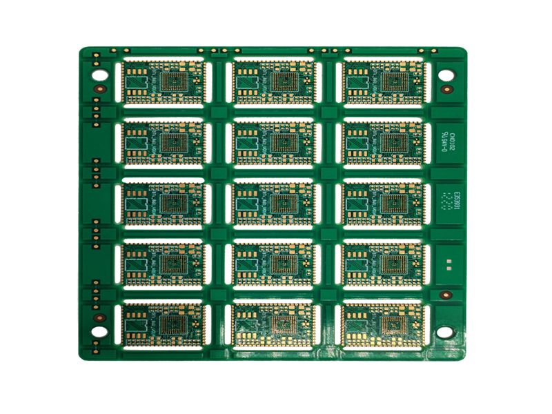
HDI 2+N+2 PCB
HDI (High Density Interconnection) circuit boards usually include laser blind vias and mechanical blind vias; general buried vias, blind vias, stacked vias, wrong vias, cross blind buried holes, through vias, blind via filling plating, thin line small gaps, Pads in microvias and technique to realize the conduction between the inner and outer layers, and usually the diameter of the blind buried is not more than 6mil.
Contact Us Send Email fiona@beton-tech.com to Us2+N+2 has the alignment, the hole punching and copper plating problem. HDI 2+N+2 has many designs:
The positions of each stage are staggered, and when connecting the next adjacent layer meed to connect through with a wire in the middle layer. The method is equivalent to two 1+N+1 HDI boards.
1+N+1vias overlap, and realize 2+N+2 by superposition, and the processing is similar to two1+N+1 holes.
Drilling directly from the outer layer to the L3 (or N-2 layer), the process is much different from the previous one, and the difficulty of punching is also greater.
HDI 2+N+2 PCB Stackup
Conventional2+N+2 (2+4+2) Stackup
Conventional secondary laminated HDI printed board (secondary laminated HDI 8 layers board, stackup is (1+1+4+1+1 or 2+4+2).
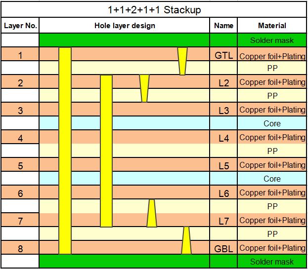
The structure of this type of board is (1+1+N+1+1), (N≥2), this kind of stackup is the mainstream design of the second stackup in the industry, and the inner multi-layer board has buried holes, It takes three presses to complete. The main reason is that there is no stacked hole design, and the production difficulty is normal. If the buried hole optimization of the (3-6) layer can be changed to the buried hole of the (2-7) layer as mentioned above, one pressing can be reduced and the optimized process to reduce costs.
Other Conventional 2+N+2 (2+4+2) Stackup
Other 1 conventional secondary laminated HDI printed board (secondary laminated HDI 8-layer board, stackup is (1+1+4+1+1or 2+4+2).
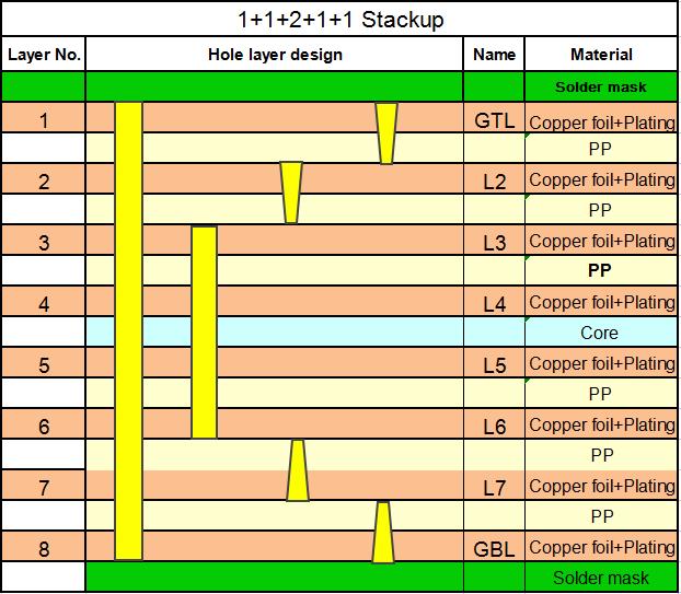
This HDI board type(1+1+N+1+1), (N≥2), although HDI board type(1+1+N+1+1) is the secondary laminated structure , but because the buried vias position is not between L3-L6 , but between L2-L7, this buried vias design can reduce the lamination once, so the secondary laminated HDI circuit board needs 3 times laminated process to optimize to 2 timeslaminated process. And this buried vias kind has another difficulty in making, there are L1-L3 blind vias, which are split into L1-L2 and L2-L3 blind holes to make.L2-L3 inner blind hole is made with hole filling. So during design process for conventional secondary lamination,our engineer advice not to use stacked hole design as much as possible, and try to convert L1-L3 blind vias into staggered L1-L2 blind holes and L2-L3 Buried (blind) holes.
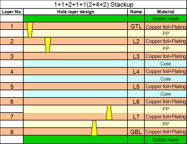
2+N+2 (2+4+2) Stackup with Cross-layer blind via
Double laminated HDI with cross-layer blind hole design (secondary laminated HDI 8 layers board, stacked structure is (1+1+4+1+1)or 2+4+2)

The structure of this type of hdi board is (1+1+N+1+1), (N≥2). This structure is a secondary laminated board that is currently difficult to manufacture in the industry. Buried holes in the L3-L6 inner multi-layer board, which needs to be pressed three times to complete. The main reason is that there are cross-layer blind vias designs, which are difficult to manufacture. Without certain technical capabilities, many suppliers cannot make such secondary laminate parts. Our HDI Factory can do this cross-layer blind vias HDI PCB.Our engineer will advice for such cross-layer blind holesL1-L3, optimize the split For L1-L2 and L2-L3 blind vias, this splitting blind holes is stacked hole splitting, but the splitting and staggered blind holes will greatly reduce the production cost and optimize the Production Process.
2+N+2 (2+4+2) Stackup with Cross blind via
L3-L6 is pressed together first, and the outer layer L2 and L7 are laminated, and punched a laser hole. Laminate L1 and L8 on it and make another laser hole. This cross blind via HDI PCB need to punch laser holes twice. Please see the stackup.
Other layer 2+N+2 Stackup
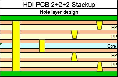
6 layers 2+N+2(2+2+2) )Stackup
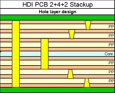
8 layers 2+N+2(2+4+2) Stackup
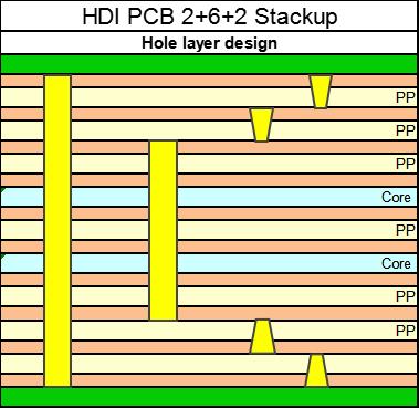
10 layers 2+N+2( 2+6+2) Stackup
High Density Interconnector ( HDI) PCB 2+N+2 Manufacturing Processing
The 2+N+2 manufacturing process is One more Copper Reduce process to pressing process than 1+N+1.One cycle is add a type.The Type II HDI board(2+N+2) manufacturing process can be divided into two types according to the drilling method.a. Using RCC and prepreg lamination, direct UV-CO2 laser drilling. b. Etching the window with chemistry and Drilling vias with a CO2 laser.

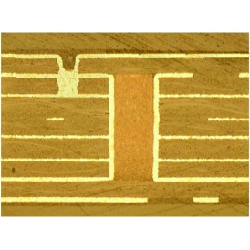
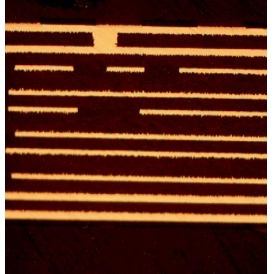
HDI Circuit Board Typical Microsection Diagram (2+N+2)
8 Layers HDI 2+4+2 Microsection | 10 Layers HDI 2+6+2 Microsection |
|
|
PCB 2+N+2 hdi circuit board technology is an improvement on the 1+N+1 HDI PCB board technology. Beton circuit 2+N+2 HDI high-speed PCB circuit board is printed and processed by Rogers RO4350B+TUC mixed pressure technology. HDI high-speed PCB circuit board is One of the series of TypeⅡHDI PCB boards produced and processed by Beton proofing and mass production, it is manufactured by Rogers RO4350B+TUC TU872SLK. This type of 2+N+2 HDI high-speed PCB circuit board is widely used in the field of aerospace and military industry.