Any layer HDI PCB
The next technological development after HDI microvia PCBs is the use of HDI any layer PCBs, where all electrical connections between layers are made using laser-drilled microvias. Any layer is the highest density plate type in HDI.
Contact Us Send Email fiona@beton-tech.com to UsAny layer HDI, also known as ELIC, is Every Layer Interconnect HDI, where each layer is a microvia-based HDI layer, and all connections between layers are made using copper-filled microvias. An ELIC is a form of printed circuit board with many interconnects and takes up minimal space, using stacked copper-filled microvias to connect multiple layers in the PCB. This any layer stackup way removed the need for PTH for surface-to-bottom connections, because both outer layers can be connected using stacked or staggered copper-filled microvias. Every Layer Interconnect HDI allows for higher component densities by utilizing a large portion of both surfaces.
Now 5G communication technology has been fully rolled out in the world. The 5G communication circuit board is highly integrated, and the PCB space cannot be increased, resulting in denser PCB traces, narrower trace width and spacing, narrower aperture and center distance, and thinner insulation layer thickness. However, the traditional HDI process has limited capabilities and is difficult to meet the needs of 5G. Therefore, any layer of HDI is also constantly researching and developing, and investing in high-tech industries.
Any layer HDI PCB Stackup
Any layer HDI PCBs all can be designed as a core-based PCB. Because Every Layer Interconnect HDI PCBs don't have any Plating through holes (PTH), and then not require any drilling holes after lamination. At building with ELIC HDI, each HDI layer stacked on either side of the core is as a separate circuit. In each HDI PCB layer, drilled microvias, filled and plated, printed and etched, and finally laminated. If other layers are to be stacked on top, they go through the same process: drilling, filling, plating, printing, etching and lamination.
Each layer of any layer HDI is a laser hole, and each layer can be connected together.
Please see the bellow 6 layers any layer HDI Stackup.

We can see the 6 layers all layer is connected together.And this microvias are stacked, which is laser stacked vias.
Our Anylayer HDI capability
Thin line capability: mass production 40/40um, research and development 35/35um;
Alignment ability: 14L arbitrary interconnection, laser microhole D+5mil;
Thin core board capacity: 50um thin core; 1027/1017 PP build-up layer; 10L arbitrary layer interconnect product board thickness 0,55mm;
Laser aperture: any layer interconnection X-VIA Min 50um;
BGA Pitch: 0.35mm;
Other Any layer stackup
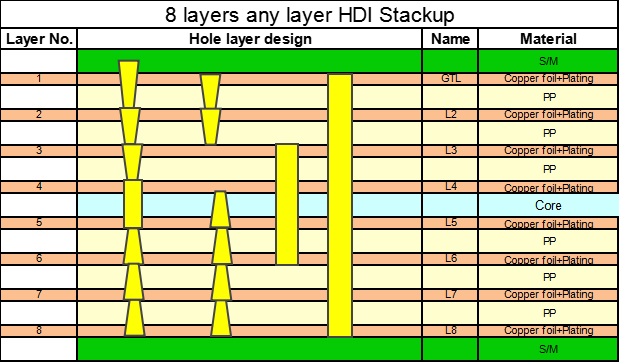
8 layers any layer HDI Stackup
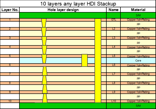
10 layers any layer HDI Stackup
Any layer HDI printed circuit board expertise:
Edge plates for grounding and shielding
Minimum track width and spacing for mass production is approx 40 mm
Stacked microvias (copper plated or filled with conductive paste)
Countersink, deep milled hole or cavity
Solder resist in blue, green and black colors.
Low halogen products in high and standard TG range
Low DK Content for Portable Devices
All reputable surfaces used in the printed circuit board industry are accessible.
The use of HDI any-layer PCBs is growing every day, especially in IoT devices due to their low price and other advantages. With advances in automated industrial equipment, IoT devices are becoming more prevalent in manufacturing, warehousing, and other industrial settings. Many of these high-tech projects include HDI technology. The next technological development after HDI microvia PCBs is the use of HDI any-layer PCBs, where all electrical connections between layers are made using laser-drilled microvias. The ability to link freely at all levels is the main advantage of this technology. Beton PCB uses copper-plated laser-drilled microvias to make these boards.
If you want to know more about any layer HDI Technology, please contact us at cathy@beto-tech.com. We have professional engineers to give you best suggestions.