2+4+2 HDI PCB for Mobile Phone
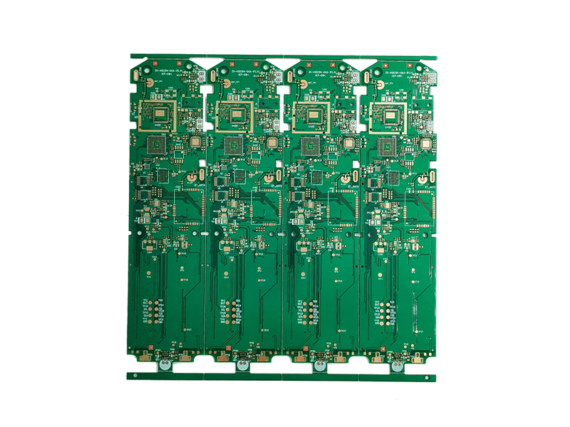
2+4+2 HDI PCB for Mobile Phone
2023-02-11
Layers: 8 Layers
Board thickness: 0.8mm
Panel Size:240*100/4
Plate material: FR4 ITEQ
Order: 2
Copper Thickness:0.5OZ
SurfaceFinish: ENIG+OSP
Line width/spacing: 2.0mil/2.0mil
Special process: 2+N+2 blind hole 1-2,1-3,6-8,7-8
Customer background
Company Location:India
Application:Moblie Phone
Field: Consumer electronics
Service:HDI 2+N+2 PCB prototype
Project challenge
2+4+2 HDI PCB for Mobile Phone adopts high TG, high speed, high frequency, thick copper, and thin dielectric layer ITEQ special material. The customer has put forward high requirements for internal circuit production and graphic size control. The width and line spacing are small, the open circuit and short circuit increase, and the yield may be relatively low. There are many thin-line signal layers, and the probability of AOI leak detection in the inner layer increases. The inner core board is thin, easy to wrinkle, poor exposure, easy to curl when etching machine.
How to Serve
Our engineering personnel check the customer's documents for the process flow of the blind buried hole plate, carefully distinguish the specific blind buried structure of the customer, and design and manufacture the working gerber according to the structural mode provided by the specification.
2+4+2 HDI PCB for Mobile Phone needs to go through 3 times of lamination. For the first time, L3-L6 is pressed, and then through holes are drilled to form electrical conduction through sinking copper and board electricity. The second time is to press the previously laminated L3-L6 sub-boards with copper foil, form high-density interconnections through laser drilling, hole filling and electroplating, and form L2-L8 sub-boards through micro-etching to reduce copper and inner layer graphics; Finally, the L2-L8 sub-board is pressed together with the copper foil to obtain a complete PCB. And the2+4+2 HDI PCB for Mobile Phone stackup is as follows.

Results and Benefits
The impedance line width of each layer is controlled within the set range, and there is no out-of-tolerance phenomenon; the impedance value is controlled within the set range of ± 10%, and the performance is qualified.
Make slices for reflow soldering and thermal stress testing to check product reliability, test conditions and results. The test results show that all slices have no adverse phenomena such as delamination, cracking, white spots, blistering, and discoloration, and the reliability test is qualified.
Customer is very satisfied with our manufacturing 2+4+2 HDI PCB for Mobile Phone. And the HDI board test all are fine. After he changed some a little, and please the mass production order to us.
HDI board production control points
Compression expansion and contraction
Buried plug hole fullness
Blind Hole solder mask opening Alignment
Line film expansion and contraction
Laser drilling roundness
Blind Hole Removal
Any HDI (High Density Interconnector PCBs)projects need production please contact us freely!Email address: cathy-beton-tech.com. BETON HDI PCBs factory focus on HDI Board (High Density Interconnect PCBs) for over 18 years, and we have strict quality control process for HDI (High Density Interconnect PCBs) manufacturing, so choose BETON PCBs factory for HDI production will save you lots of time, cost and energy.