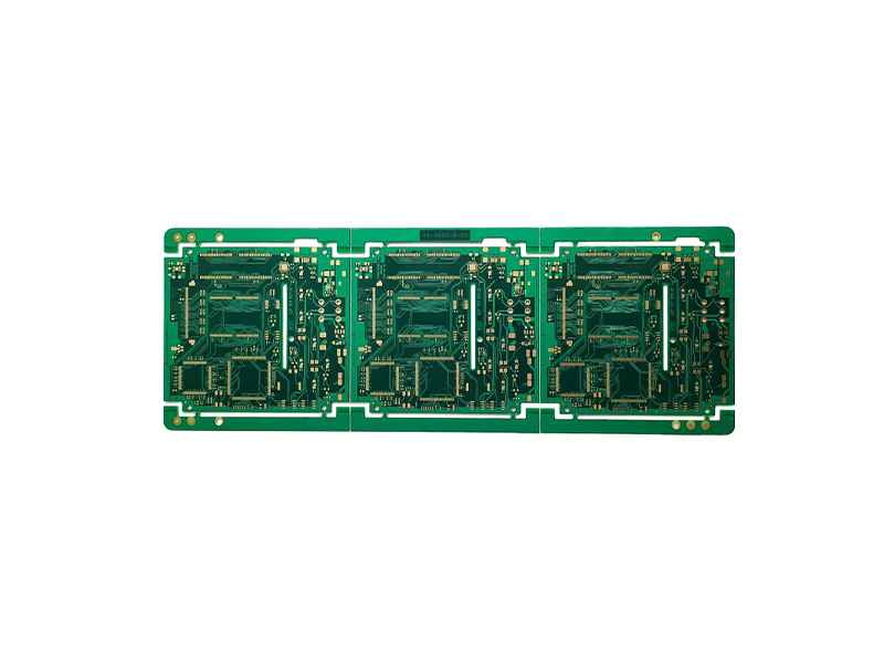
10 layers 3+N+3 HDI PCB for Medical device
10 layers 3+N+3 HDI PCB for Medical device
2023-02-11
Layers: 3+4+3
Material: FR4 Tg170
Plate thickness: 1.2mm
Panel size: 126*118mm/4
Outer layer copper thickness: 35um
Inner layer copper thickness: 18um
Minimum through hole: 0.20mm
Minimum blind via: 0.10mm
Minimum BGA: 0.25mm
Line width and spacing: 2.8/3.2mil
Surface treatment:ENIG2U+OSP
Send Email: fiona@beton-tech.com to UsCustomer Background
Company Location:Switzerland
Application:Blood glucose meters, electrocardiographs, CT scan systems, blood pressure,MRI scan system
Field:Medical device
Service:PCB Prototype, PCB Manufacturing
Project Background
It is a medical device company based in Switzerland. Their medical equipment requires 10 layers 3+N+3 HDI PCB.
The customer's previous HDI design was 2+N+2 stackup, but now it needs 3+n+3 to re-adjust the differential impedance. At the same time, it is difficult for him to find a suitable HDI factory due to the increasing difficulty of 3+n+3 HDI PCB production. The 3+n+3 prototype tests that his previous suppliers could do were not good enough to work on his medical equipment.
In view of the above situation, the customer needs to find a new supplier who can control the performance of HDI and meet the differential impedance requirements without changing the original drawings. At the same time, due to his former supplier's serious delay in delivery, now the project is urgent, and the customer wants to provide samples within 8 days.
By chance, the customer searched our website through Google and learned that we can make difficult HDI boards, and even any layer HDI pcb, so he sent us the gerber information. Considering the customer's urgent needs, we prioritize this order and send the quotation to the customer within half an hour. After checking the design files, our engineering team also quickly provide EQs and working gerbers to customers for confirmation.
It takes about 1 day from receiving the inquiry to production approval, and the sample is also completed within 8 days, the quality is very good, and the 3+n+3 HDI pcb also performed very well in his medical equipment test, so it has been well received by customers.
Project Challenge
The process of 10 layers 3+N+3 HDI PCB is much more complicated. Laminate layers 4-7 first, then L3 and L8, L2 and L9, making well-made blind/buried vias, and finally L1 and L10, making well-made vias. It takes 4 lamination times, so none of the customer's previous PCB manufacturers could make it.
How to serve
We have a complete HDI equipment production line, various advanced equipment, and a dust-free workshop. Customers need FR4 TG170 material, and we have enough TG170 material raw materials in our warehouse to meet customers' urgent requirements.
HDI circuit board glue inspection, manual inspection of glue point diameter. Use X-barRchart to record results
Our QC team will check the HDI circuit board glue before shipment, and manually check the glue dot diameter. Use X-barRchart to record results
Our sales and engineering teams are on call 24 hours a day to solve customer problems in a timely manner, ensuring that any questions raised by customers can be responded quickly, and ultimately improve the work efficiency of customers and our production department.
Results and Benefits
The 10 layers 3+N+3 HDI PCB prototypes we manufactured meet customer performance and delivery time requirements. Our company has enough TG170 plates, so when EQ confirms it is good, we can start production immediately. Finally, complete the entire HDI PCB production as required within the specified time.
The excellent performance of HDI PCB ensures that the assembly of the customer's final product can also be carried out smoothly and stably, which greatly shortens the communication time and delivery time of the customer. Customer terminal assembly and production efficiency has been greatly improved.
Multi-order blind vias realize layer-to-layer interconnection
Staggered via interconnection method
|
Resin plugging method
|
Filled Copper Stacked Via Interconnection
|
Cross-layer interconnection method
|


With the rapid development of HDI PCB technology, the requirements for the production of multi-level HDI boards with stacked holes will become more and more stringent, which poses more new challenges for us. The key technology of this kind of stacked HDI board production is still the alignment accuracy between layers, fine lines and electroplating hole filling, etc. Our engineers are also constantly learning about the production technology of this type of board, constantly summing up experience and accumulating results, Gradually improve our process level for making multi-level HDI boards with stacked holes.
Any 3+n+3 HDI PCB needs, please feel free to contact us at cathy@beton-tech.com. We have professional HDI engineers to help you build up your HDI PCB products.