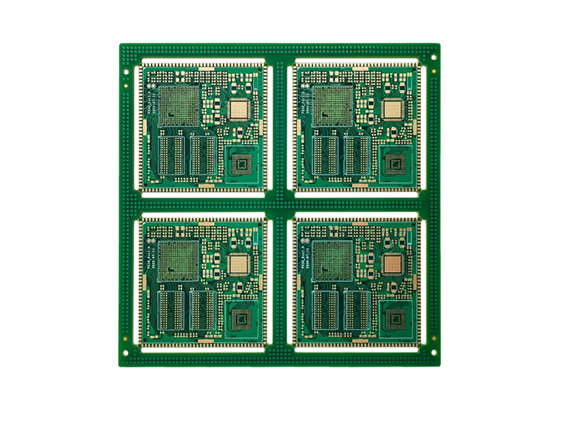
1+4+1 HDI PCB with Castellated hole
1+4+1 HDI PCB with Castellated hole
2023-04-25
Material: FR4 Tg170
Board thickness: 1.2mm
Panel Size:120*96/4
Outer Cu thickness: 35um
Inter Cu thickness: 18um
MinThrough-hole: 0.20mm
Min Blind Via: 0.10mm
MinBGA: 0.20mm
Line Width/Space: 2.5/2.2mil
Finish:ENIG2U+OSP
Send Email: fiona@beton-tech.com to UsCustomer background
Company Location:Italy
Application:Communication module
Field:Telecom
Service:HDI 1+N+1 PCBManufacturing
Projectbackground
The HDI PCB is 1+N+1HDI with the Castellated hole. And the Castellated hole HDI PCB stackup is 1+4+1. Customer need the PCB Class 3 Acceptance Standard. Test method according to IPC-TM-650, +/-0.75%.
Project challenge
This 1+4+1 Castellated HDI PCB has Castellated holes on the edge of the board, and the product has copper thorns on the hole wall, and the residue has always been a problem in our processing process.
This Castellated HDI PCB with a whole row of Castellated holes on the side of the board is characterized by a relatively small hole diameter. There are copper thorns in thesehalf-metallized holes. Will cause a bridge short between the two pins.
HDI PCB is different from ordinary FR4 PCB. Customers have increasingly strict requirements on the alignment of each layer of HDI circuit boards. Usually, the alignment tolerance between layers is controlled at±75um. And factors such as dislocation superposition and interlayer positioning methods caused by the inconsistency of expansion and contraction of different core board layers make it more difficult to control the interlayer alignment of high-layer boards.
How to Serve
First, our engineers evaluate the gerber according to customer requirements, and do EQs for customer confirmation without affecting the performance of 1st type HDI PCB.
The castellated hole production first to drill the hole,thenthe second drill,shape process after the hole is formed, and finally retains half of the metallized hole. The main production process of the half-hole(castellated hole) board is the outer layer circuit design; the substrate pattern is electroplated copper; the substrate pattern is electroplated tin; Pore treatment; Film withdrawal; Etching.
The 6 layers first-order HDI Castellated hole circuit board can be laminated at one time. First, make a circuit board with L2-L5.At that time, L2-L5 buried vias has finished and add the L1 and L6 through holes to laminate. Drill L1-L6 through holes and L1-L2, L5-L6 blind vias are made into a whole circuit board.See the 1+4+1 HDI Stackup.

Results and Benefits
Beton Circuits is a professional 6 layers first-order HDI half-hole circuit board proofing batch manufacturer. We accurately grasps customer needs and every key point in the manufacturing process of 1+4+1 HDI with Castellated hole circuit board proofing, and produces 6 layers first-order HDI half-hole circuit board with zero-defects on time.
1+4+1 HDI PCB with Castellated hole is suitable for BGA with smaller ball pitch and higher I/O count, increasing routing density in complex designs, lower Dk/Df material for better signal transmission performance.
Our manufacturing 1+4+1 HDI PCB with Castellated holehas been tested with pretty good results.And Customer are applying some minor modifications before starting the first production lot.After test a week, we received the this client’s first mass production orders.
Any HDI PCB demands, please contact us at cathy@beton-tech.com. Professional engineer to help to give your suggestion and do the DFM Check.